

Sitting down to write this should be exciting. We are about to wave farewell to one of the most successful years in gaming for well over a decade. Unfortunately, 2023 is also the year the gaming industry saw mass layoffs, so it is impossible, in good conscience to celebrate fully as we might have wanted to.
Anyway, as we settle down for the holidays we can’t possibly be short of things to play, even if we don’t like Baldur’s Gate 3. CRPGs aren’t for everybody and it may not have been your own personal game of the year.
Whatever your weapon of choice is as we enter into 2024, the chances are somewhere along the way it’s been affected by layoffs and redundancy rounds. It’s important to get this out of the way before we go slapping the gaming industry on the back for a job well done in 2023.
It’s nigh on impossible to chart how many people have been “let go” (HR terminology there) this year, in some cases, as soon as the work has been done.
The events have been so seismic there is an excellent blog attempting to track them all. It’s failing, but it’s trying. As well as developers, games media has been decimated, with X awash (ironically, seeing it also removed most of its staff this year) with games journalists desperately seeking out work. Games journalists do not tend to earn a lot of money, they do it for the love of playing games, but that does not always fit into the boardroom plans. What is this AI you talk of? It can write articles for free you say? Interesting…
So the upshot of all this is that we are unlikely to see another 2023 in terms of consistent levels of gaming brilliance for some time. The cycle is complete for now.
Some of those excellent devs and writers will move off into different spheres and be lost to the industry. Bosses and CEOs will be smiling and laughing and pocketing bonuses at a job well done, certainly, if you look at the profit margin.
These future holes though are for 2024’s Year in Gaming and beyond. This year, because of so many people’s efforts, we were treated to a very special time on whatever device we chose to play on.
Let’s have a look at some of the more memorable events.
2023 – As it happened
January / February.
January 18th was the date Microsoft potentially blew games publishing apart and caused a war in the rift for the entire year when it announced its acquisition of Activision Blizzard. Obviously, that was not the end of the story.
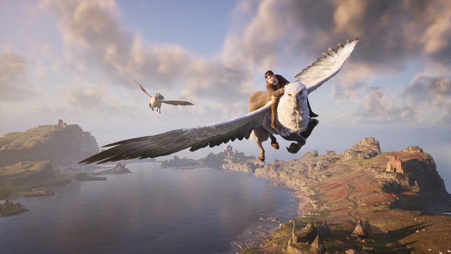
Hogwarts Legacy. Delayed but finally, here, the best game ever to feature the bespectacled boy wizard arrived to a fanfare of both love and hate. Capturing the feel and magic of JK Rowling’s bestsellers, it may not have been the best game of the year, but for many it was.
Its darker side was the boycott of many gamers who no longer felt they could support a Rowling-associated product due to her views on transgender. The politics aside, Hogwarts Legacy went on to become the best-selling game of the year, even getting a Nintendo Switch version towards the back end of 2023.
February also saw the release of the much-delayed Sons of the Forest. After the phenomenal success of The Forest, this sequel had been on many a wishlist. And while it was released unfinished in Early Access, injured sidekick Kelvin became one of gaming’s favorite characters of the year.
March / April
If we had the big hitters in the first two months of the year, the next two were a little more barren.
We did get an Open Beta of Diablo IV which allowed us to see Sanctuary in all its latest version glory, and for a beta, there was a lot to do over the two weekends we got to play.
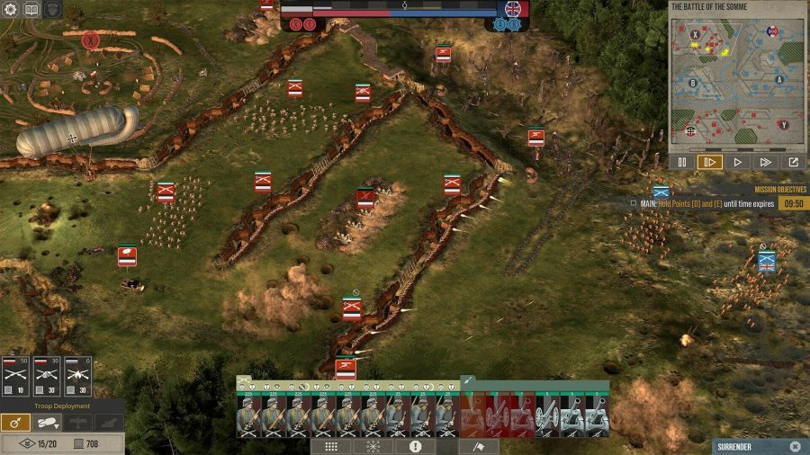
Big releases were thin on the ground. We got a return to EA Sports golfing classic PGA Tour. One of the best war strategy games in a long time, The Great War Western Front was released and managed to capture a little of the harrowing trench warfare for World War 1.
Right at the end we got a biggie though when Star Wars Jedi Survivor appeared alongside the new gacha behemoth Honkai Star Rail.
May
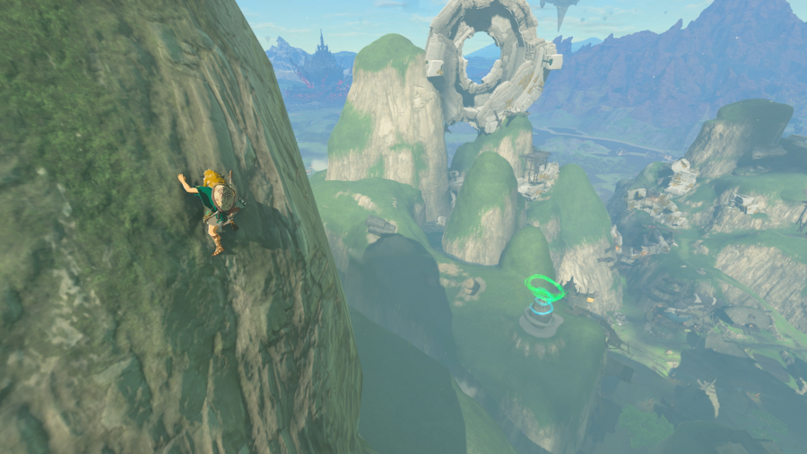
The month of May was a blur. Tears of the Kingdom dominated. Redfall and Lord of the Rings: Gollum appalled in equal measure, but other games were easy to miss if you were a Nintendo Switch owner hooked on Zelda’s latest exploits.
Age of Wonders 4 arrived as did the underrated Marvel’s Midnight Suns. We even got a new Farming Simulator. Company of Heroes 3 came out after a long hiatus from the second game in the series, which, unfortunately, it didn’t quite live up to.
But it was all about The Legend of Zelda: Tears of the Kingdom. What a game. Probably a masterpiece on many levels. As long as you liked Breath of the Wild. A rare game worth buying hardware for.
June / July
In June we got some big hitters including the PS5 exclusive of Final Fantasy XVI which sold by the bucketload as expected. June the 6th was Diablo IV day, the game finally came out and people flocked back to the grind like they had never been away. After the bad press the mobile-focused Diablo Immortal had got, it felt good to be back.
July was much quieter although platform heroes Ratchet and Clank made a gaming reappearance which was fun.
August
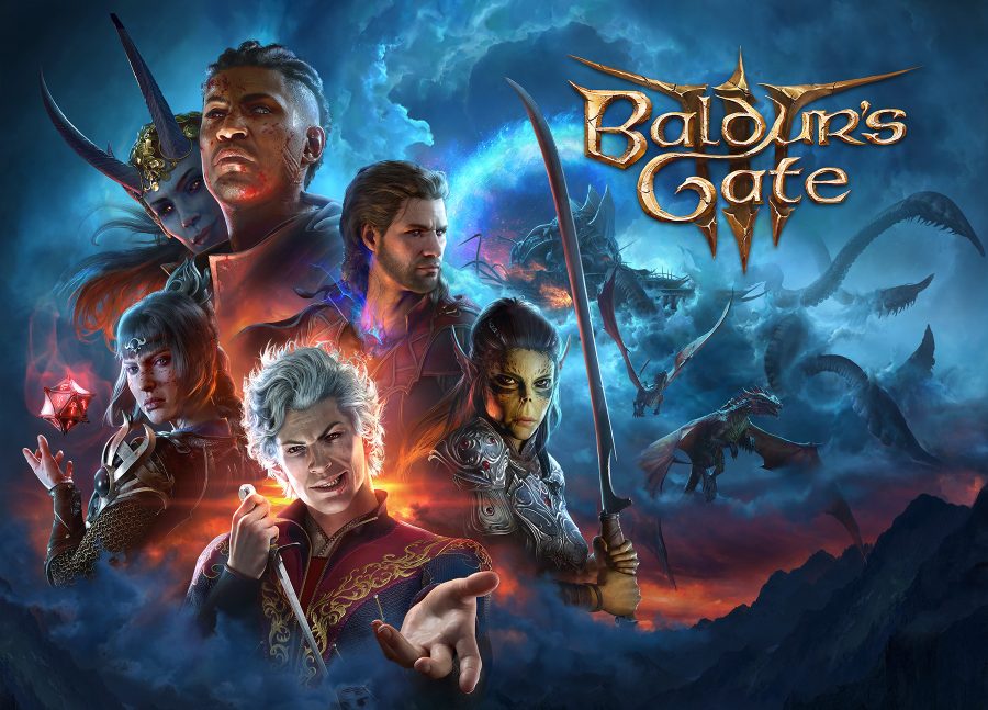
If May was the month of Zelda, August belonged to Baldur’s Gate 3. The eventual Game of the Year captivated all who played it. For a rare moment, a game captured what it was like to play a table-top D&D game. It was, and remains a stunning gaming achievement deserving of the long-term success it will get.
Sea of Stars also deserves a mention. A great throwback RPG with so many cool moments and a great narrative. Check it out if you missed it.
September / October

Ah Starfield, why do we think your star has not risen fully yet? Coming weeks after the exceptional Baldur’s Gate brought Starfield some unfair comparisons. It is not a bad game, repeat it is not a bad game. It is just not an exceptional one. Hype hurt Bethesda with Starfield but we have new content on the way in the new year. Don’t write this off just yet folks.
Mortal Kombat made a welcome return to the fighting arena, laden with DLCs and buyable extra characters. What have they done to you?
By October the bigger titles were lining up for action. Assassin’s Creed: Mirage was first, followed by Forza Motorsport for the Xbox. Lords of the Fallen surprised everyone and captured a lot of Elden Ring’s old player base.
Then in the space of five days, we got Super Mario Wonder – another Switch-seller, Marvel’s Spider-man 2 – a PS5 seller, and Cities: Skylines 2 – a bug-ridden monstrosity at launch, thankfully most of which has now already been sorted, lining it up for a stellar few years at the pinnacle of city builders.
November / December
November was quieter than you might expect. We did get Persona 5 Tactica and the hugely disappointing Gangs of Sherwood.
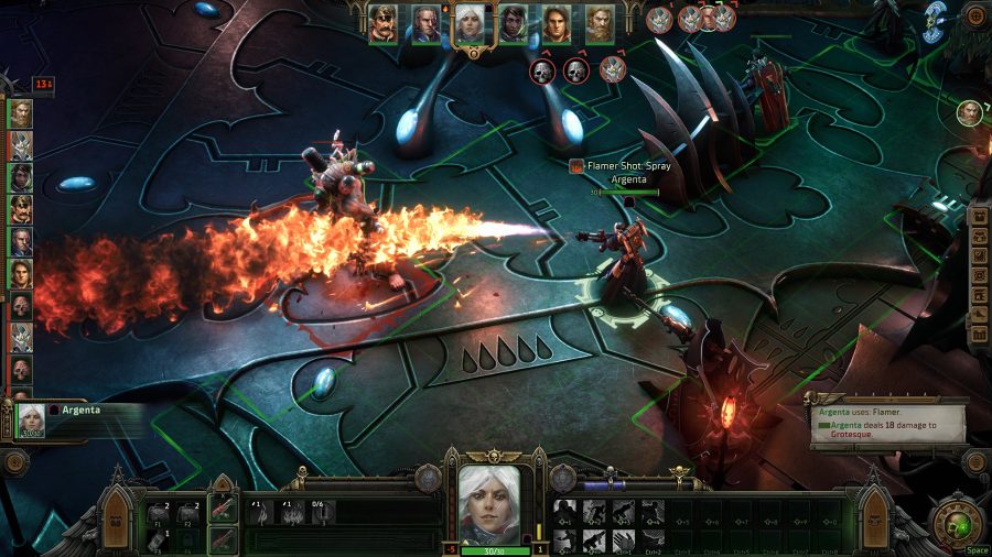
December at least provided some new fodder for our holiday breaks. Warhammer 40k: Rogue Trader was a really good CRPG that was lapped up by fans. We are definitely going to mention Lego Fortnite for sweeping all those Fortnite players into minifig heaven.
Honorable mentions for December go to the excellent city-building/survival hybrid Against the Storm and Ready or Not, which recaptured all those times playing as a SWAT officer in SWAT 4.
On the downside, Insomniac Games got hacked and had all its files stolen (not leaked!) and dumped on the internet for everybody to poke through. A sour note to end a truly bittersweet 12 months in gaming.
Same time next year?
Source link